
Custom Online Laser Micromachining
CipherFab offers advanced laser micromachining solutions for producing ultra-fine features, microstructures, and precision components across metals, ceramics, polymers, and advanced materials. Achieve superior dimensional accuracy, minimal thermal impact, and outstanding surface finish with instant DFM feedback on every design.
CipherFAB values your privacy and security. Learn More
Get an Instant Custom Online Laser Micromachining Quote
Upload your CAD FilesSupported files: STEP, STP, SLDPRT, DXF, IPT, PRT, SAT
Laser Micromachining Service
CipherFab offers a high-quality laser micromachining service using pulsed ultrashort laser systems — picosecond and femtosecond duration pulses — to ablate material at micron-scale resolution with near-zero heat-affected zone, no tool contact, and no mechanical forces on the workpiece. As a remote photonic processing technique that imparts no mechanical force on a material surface, laser micromachining is ideal for creating intricate, tight-tolerance features on small, delicate parts — enabling feature sizes and surface quality unachievable by CNC micro machining, chemical etching, or EDM. CipherFab provides instant quotes on laser micromachined components with DFM feedback on every uploaded file. HubSpot
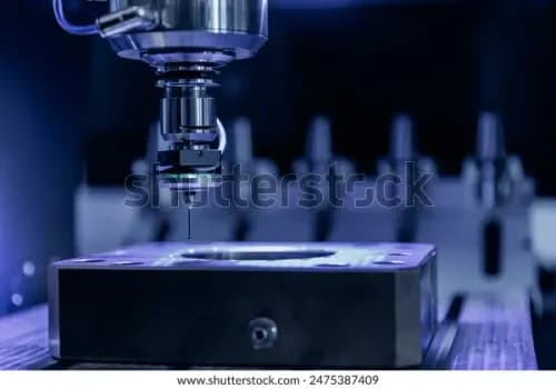
Recommended Materials for Laser Micromachining
Materials supported for this capability.
Laser Micromachining
Laser Systems Picosecond Nd:YAG (1064 nm / 532 nm / 355 nm) — metals, ceramics, polymers; tight tolerances and low HAZ Femtosecond Ti:Sapphire / Yb:KGW (800 nm / 1030 nm) — near-athermal ablation; near-zero HAZ; all materials including glass and ceramics Nanosecond UV Nd:YAG (355 nm) — PCBs, polymers, and UV-absorbing materials; cost-effective for less critical features
- Metals Stainless Steel 304 / 316L
- Stainless Steel 17-4PH
- Titanium Ti-6Al-4V (Grade 5 and Grade 23 ELI)
- Aluminium 6061
- Inconel 625
- Nickel alloys
- Cobalt-Chrome
- Tungsten
- Shape memory alloys (Nitinol)
- Ceramics & Glass Alumina (Al₂O₃)
- Silicon Carbide (SiC)
- Silicon Nitride (Si₃N₄)
- Borosilicate Glass
- Quartz (fused silica)
- Sapphire
- Zirconia (ZrO₂)
- Semiconductors Silicon wafer
- Gallium Arsenide (GaAs)
- Germanium
- Silicon Carbide (SiC) for power electronics
- Polymers & Composites PEEK
- Polyimide (Kapton)
- PTFE
- LCP (Liquid Crystal Polymer)
- FR4 PCB laminate
- Carbon Fibre Composite (CFRP)
- Kevlar composite
Laser Welded Assemblies
Assembly Types Supported Hermetic enclosures and sensor housings — continuous seam weld for full IP67/IP68 seal integrity Medical device components — laser spot and seam welding of stainless and titanium surgical instruments Battery tab and busbar joining — pulsed fibre laser welding of aluminium, copper, and nickel tab materials Automotive structural sub-assemblies — high-speed robotic laser seam welding of body panels and structural frames Precision thin-wall tube assemblies — lap and butt seam welding of thin-wall stainless and titanium tube Electronics enclosures — hermetic seam welding of stainless and Kovar housings for sensor and RF applications
- Metals — Fibre Laser (1.064 µm) Stainless Steel 304 / 304L
- Stainless Steel 316 / 316L
- Stainless Steel 17-4PH
- Mild Steel 1018
- Galvanised Steel G90
- Aluminium 5052
- Aluminium 6061
- Aluminium 7075
- Titanium Ti-6Al-4V
- Inconel 625
- Inconel 718
- Copper 110
- Nickel 200 / Nickel 201
- Kovar
- Invar
Tolerance Standards for Laser Micromachining
General tolerance information for this capability.
Laser Micromachining
| Description | General Tolerance |
|---|---|
| Minimum Feature Size | 1 µm (femtosecond laser) — 5 µm typical production minimum |
| Standard Positional Accuracy | ±2.5 µm with vision alignment — picosecond and nanosecond systems |
| High-Precision Positional Accuracy | ±0.5–1.0 µm — femtosecond systems with integrated vision alignment |
| Surface Roughness (as-ablated) | Ra < 0.1 µm achievable with femtosecond pulses |
| Heat-Affected Zone | < 1 µm — femtosecond pulses; < 5 µm — picosecond; 10–50 µm — nanosecond |
| Hole Aspect Ratio (max) | Up to 20:1 on microchannels and micro-holes |
| Inside Corner Radius | < 3 µm achievable — femtosecond laser |
| Taper | Near-zero taper on through-features with femtosecond trepanning |
| Edge Condition | No burr; no dross; no mechanical distortion |
| Recast Layer | < 1 µm — femtosecond; < 3 µm — picosecond |
| Feature Repeatability | ±1 µm across production batch |
| Laser Micromachining — Process Capabilities | Process |
| Feature Size | Typical Tolerance |
| Best For | Laser micro-drilling |
| 1 µm–500 µm dia | ±1–5 µm |
| Micro-vias, filter screens, cooling holes, nozzle orifices | Laser micro-cutting |
| 5 µm kerf width | ±2.5 µm |
| Stent cutting, thin foil profiling, sensor membranes | Laser micro-milling |
| 5 µm feature | ±2.5 µm |
| Microfluidic channels, surface texturing, optical structures | Laser scribing |
| 1 µm line width | ±1 µm |
| Wafer dicing, solar cell scribing, display glass scoring | Laser surface texturing |
| Sub-µm Ra achievable | ±5 µm depth |
| Implant surface osseointegration, tribological texturing | Laser ablation marking |
| 5 µm resolution | ±2 µm |
Laser Welded Assemblies
| Description | General Tolerance |
|---|---|
| Weld Bead Width (minimum) | 0.1 mm (100 µm) |
| Weld Seam Positional Accuracy | ±0.05 mm with integrated seam tracking |
| Heat-Affected Zone | 0.5–1.0 mm typical — narrowest of any fusion welding process |
| Dimensional Tolerance (post-weld) | ±0.010″ — tighter than arc welding processes |
| Distortion | Minimal — low heat input prevents bulk thermal distortion |
| Weld Penetration | Up to 12 mm single pass — material and power dependent |
| Material Thickness Range | 0.1 mm to 12 mm |
| Weld Quality Standard | ISO 5817 Level B (high quality) as standard |
| AWS Standard | AWS D1.1 (steel) · AWS D1.2 (aluminium) |
| ASME Standard | ASME Section IX for pressure-critical sealed assemblies |
| Hermetic Seal Test | Helium leak test available — leak rate < 1 × 10⁻⁸ mbar·l/s achievable |
| NDT Options | Visual · Dye penetrant · Ultrasonic · Radiographic · Helium leak test |
Design Guide: Laser Micromachining
We have compiled our best tips into this guide to help you understand laser micromachining processes, how to design micro-features for reliable laser production, minimum feature sizes by laser type and material, aspect ratio limits for micro-holes and channels, surface condition and reflectivity management, workholding strategy for small and delicate components, femtosecond versus picosecond process selection guidelines, and how to specify positional tolerance, feature size, surface finish, and inspection requirements for laser micromachined components.
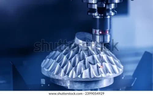
Advantages of Laser Micromachining
Laser micromachining achieves finer features down to 1 µm and tighter tolerances of ±1–5 µm than conventional methods, without tool wear or mechanical forces — and it excels with heat-sensitive materials. For medical device components, surgical instruments, implants, and catheters — implantable medical devices such as stents, intraocular lenses, prosthetics, and catheters are becoming increasingly complex and feature sizes are shrinking to address new usages and improve patient outcomes — laser micromachining produces features below 100 µm with the surface quality and dimensional consistency that neither CNC micro machining nor chemical etching can achieve at this scale. The features must be extremely precise with tolerances as small as ±2.5 µm, and there is very little room for defects — laser beams can be focused to extremely small diameters, and since they are pure light, there is no chance of broken or worn tools causing inconsistent results. CipherFab's laser micromachining service covers metals, ceramics, glass, silicon, and polymers — across micro-drilling, micro-cutting, micro-milling, scribing, and surface texturing — with instant online pricing and DFM feedback on every upload.



Start Your Laser Micromachining Project Today
Get Free Instant QuoteUpload your CAD files for an instant quote with DFM feedback on every order.